Stanford Researchers Use Diamonds To Build World's Thinnest Nanowires

Researchers at Stanford University and the Department of Energy’s SLAC National Accelerator Laboratory have recently developed a technique to build the thinnest possible nanowires which conducts electricity. Diamondoids, also regarded as the world’s smallest pieces of diamonds have been used to create such nanowires, having as small as three atoms wide. These nanowires find application in creating fibers that can be used in optoelectronic devices, electricity-generating fabrics and in designing superconductors that suffer minimal energy losses. Hao Yan, a Postdoctoral researcher at Stanford University and one of the brains behind this research explained the full details of his work in the paper titled ‘Hybrid metal –organic chalcogenide nanowires with electrically conductive inorganic core through diamondoid –directed assembly’ which has been published in the journal Nature Materials.
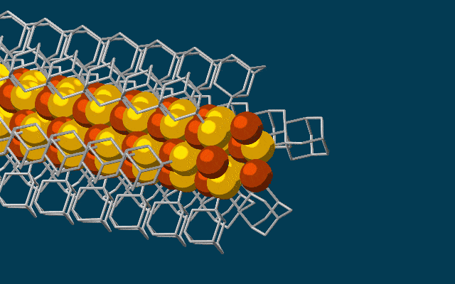
LEGO Nano-wire Clusters in Action - Each Block Consists of a Diamondoid (Grey), Sulfur (Yellow) and Copper (Brown) Atoms, GIF Credits - #-Link-Snipped-#
Adamantane – the smallest possible diamondoid, has been used to build the conductive nanowires. It consists of 10 carbon atoms bonded together in a cage like structure. It is then attached to a sulfur atom which further bonds with a copper ion in a solution to build the nanowire block. Because of the Van der Waals force, the diamondoids attract each building blocks, thus, self-assembling to form the nano-wire structure. Much like that of the LEGO blocks, these building blocks only assemble depending on their shape and size, thus it has also been named as LEGO-nano wires. Copper and sulfur atoms form the core of these nano-wires whereas the diamondiods act like an insulator, forming the cladding.
The team has further used elements like Zinc, Cadmium and Silver to develop wires which can be perceived through naked eye and have been successfully used in piezoelectric devices, LED, etc. Scientists are now aiming to improve the performance of these wires in order to enlarge their application domain and use them in designing tiny electronic devices and photonic gadgets.
Source - #-Link-Snipped-#
0