

What PCB Design Issues Do You Usually Discover Only After Manufacturing?
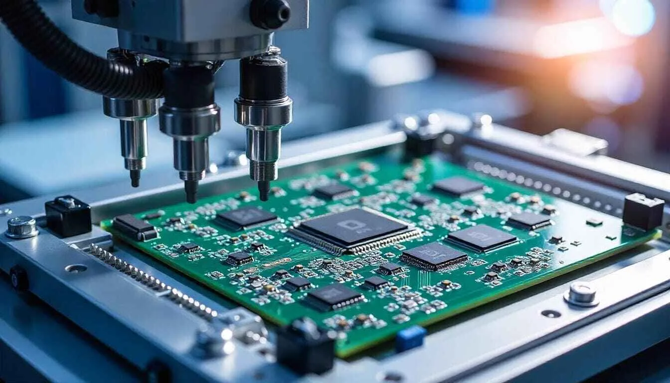
What PCB Design Issues Do You Usually Discover Only After Manufacturing?
Designing a PCB that works in simulation or during the initial prototype stage doesn't always mean everything will go smoothly during manufacturing and assembly.
Sometimes, small design decisions can create unexpected problems later. Incorrect footprint dimensions, insufficient spacing, poorly positioned vias, solder mask issues, or inadequate component clearances can all affect the final board.
One thing I've noticed while exploring PCB design and manufacturing is that some problems are easier to prevent during the design stage than to fix after fabrication.
PCBCool, which provides PCB manufacturing and assembly services, also covers practical PCB engineering topics that highlight the importance of considering manufacturability alongside circuit functionality.
I'm curious about the experiences of other engineers here:
What is the most common PCB design mistake you've encountered during fabrication?
Do you follow specific DFM (Design for Manufacturability) checks before sending your Gerber files to a manufacturer?
Have you ever had a PCB that worked perfectly in the prototype but developed issues during actual assembly?
Would be interesting to hear some real-world experiences, especially from engineers who regularly work with multilayer boards and complex designs.