Scientists Discover New Way To Manage Electrons In Slim Semiconductors

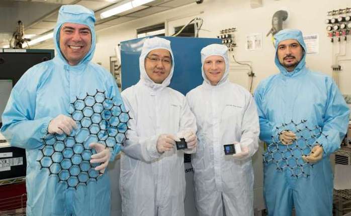
In a recent research, a team from National University of Singapore (NUS) has demonstrated a new way to control electrons by confining them in a device made out of atomically thin materials and applying external electrical and magnetic fields to them. The work comes through after two years of research, with the ultra thin semiconductor material - in this case, titanium diselenide coated with boron-nitride, being almost 100,000 times thinner than a strand of human hair.
Almost all the modern technology inventions as semiconductors, light bulbs, motors etc. run on electricity accessing the flow of electrons through devices. However directing their movement isn’t easy, as they move rapidly fast and have same electrical charge owing to which they repel each other.
To control the electron behaviour in semiconductors, a ‘chemical doping’ technique is required, where small amount of a foreign substances are embedded in the material to either release or absorb electrons. This creates a change in electron concentration which is further used to drive electric currents.
The chemical doping technique though has its own fall outs. It causes irreversible chemical change in the material being studied; the foreign material embedded often veils the electronic states of pure material.
In the new study, the researchers were successful in imitating the effects of chemical doping by replacing the technique, with the external application of electrical and magnetic fields; to the atomically thin material, titanium diselenide (TiSe2), encapsulated with boron-nitride (hBN). The thinness of the two materials was the key here, as it helped confine the electrons to a two-dimensional layer over which the fields had uniform and optimum effect.
The researchers were even successful in driving the material into the state of ‘superconductivity’, where the electrons move without any loss of energy or heat.
The new breakthrough would help enhance the performance of electrical devices. They would have obvious advantages over traditional superconductors, in applications such as smaller, portable magnetic resonance imaging (MRI) machines.
Next natural step of progression for the scientists is development of high-temperature two-dimensional superconducting materials. Current materials require an extremely cold temperature of -270°C to function, hence making it impossible to have applications such as loss-less electrical lines, levitating trains and MRI machines.
The phenomenal leap is sure to bring forth more progress in coming future in the field of solid-state phenomenon and high-temperature superconductivity.
Source: #-Link-Snipped-#
0