
NASA To Build World’s First Integrated Photonics Modem
NASA has been reportedly developing the worldâs first integrated-photonic communication modem, that would eventually power various sectors including telecommunication, imaging, and manufacturing. The IP modem will be tested above the earthâs surface, in the International Space Station by the year 2020. NASA explained this new expedition is an integral part of NASAâs multi-year Laser Communications Relay Demonstration aka LCRD.
Once placed and set to work, LCRD LEO (Low-Earth Orbit) User Modem and Amplifier (ILLUMA) will expectedly demonstrate record performance in high-speed laser-based communications. Since 1958, NASA relied on Radio frequency based communication. According to Don Cornwell, director of NASAâs Advanced Communication and Navigation Division within the space Communications and Navigation Program, owing to high demanding data rates, the advancement of technology became crucial and eventually led to the newest IP based modem. The tiny device is stuffed with coherent optical sources such as Lasers, switches and wires which are all embedded on a microchip similar to IC technology. LCRD modems will use lasers to encode and transmit data at rates 10 to 100 times faster than other contemporary technologies.
The lesser mass and power requirements along with higher data speeds would help in producing high-resolution videos and measurements taken from spacecrafts on planets across the solar system. ILLUMA is an emerging technology based on integrated photonics that replaces standard fibre optic cables used for internet communication.
Similar to electrons in integrated circuits, IP circuits make use of photons as the carrier element of circuits. Recent developments in nanostructures, meta-materials and silicon technologies expanded the range of application for IP chips.
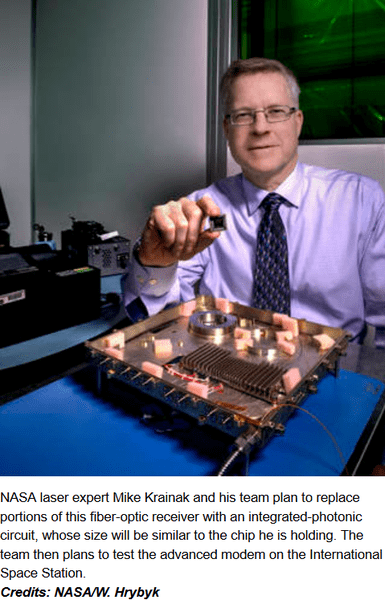
Mike Krainak, leader of the modemâs development team at NASAâs Goddard Space Flight Center in Greenbelt at Maryland explained that the new technology would produce communication systems with enhanced reliability and better functionality. Their main goal is to produce low-cost, high-volume, manufacturing methods to merge electronic integrated circuits with integrated photonic devices.
Krainak added that switching to photonics will eventually improvise space craft equipments and the study of planetary sciences. The concept could also be implemented in intra-Earth communication to ultra-modernize the contemporary systems. He has claimed that due to such a board spectrum of advantages tech giants like Google and Facebook are also considering about transforming to IP technology.
Watch Boson sampling using integrated photonics circuits:
Source: #-Link-Snipped-#