
Barrier Potential of PN junction diode
Determination of Barrier Potential V0 in p-n junction
Or
Contact difference V0 in p-njunction
Or
Boltzmann Relationship
(Asked many a times in exams)
1. Consider a p-type of semiconductors with non-uniform concentration(graded)i.e. there exist a concentration gradient.
2. Let the bar be open circuited. Therefore total current because of hole is zero.
Jp = Jpdrift +Jpdiff……………………………….(drift current and diffusion current)
pqµpE = qDp (dp/dx);
Thus, E=(1/p)(Dp/µp)(dp/dx);
According to Einstein Relationship
(Dp/µp)=VT =volt equivalent of temperature
E= (1/p) VT (dp/dx);
- (dv/dx) = (1/p) VT (dp/dx);
dv = - (VT/p) dp
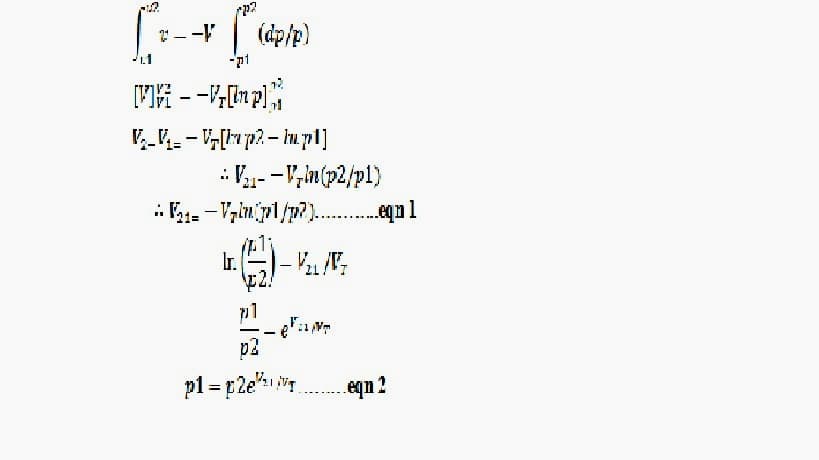
Integrating on both sides:
Now consider a p-n junction bar whose half side is doped with accepter impurity causing p-type material and other half is doped with donar impurity causing n-type material.
![[IMG]](proxy.php?image=http%3A%2F%2Fwww.crazyengineers.com%2Ffile%3A%2F%2F%2FC%3A%2FUsers%2Fa%2FAppData%2FLocal%2FTemp%2Fmsohtmlclip1%2F01%2Fclip_image022.gif&hash=a2ffab29ead909fe1bae19da49e9c32e) on p-side, p1=pp =NA= Accceptor ion concentration……..eqn 3
on p-side, p1=pp =NA= Accceptor ion concentration……..eqn 3
Similarly on n-side, nn = ND
pn = ni2 / ND
and we have p2= pn = ni2 / ND ……….eqn 4
V21 is the potential existing across the junction which can be identified as the barrier potential denoted by V0
Put 3 and 4 in eqn 1, we get
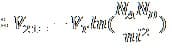
![[IMG]](proxy.php?image=http%3A%2F%2Fwww.crazyengineers.com%2Ffile%3A%2F%2F%2FC%3A%2FUsers%2Fa%2FAppData%2FLocal%2FTemp%2Fmsohtmlclip1%2F01%2Fclip_image024.gif&hash=58c22402e86c111fa7f74941cef9786f)
Thus this is the expression for barrier potential