CrazyEngineers
  • What's Inside The SD Card ? How SD Card Works ?

    Abhishek Rawal

    Abhishek Rawal

    @abhishek-fg9tRh
    Updated: Oct 22, 2024
    Views: 1.1K
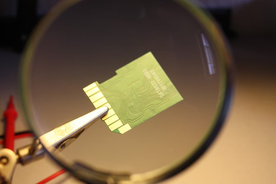
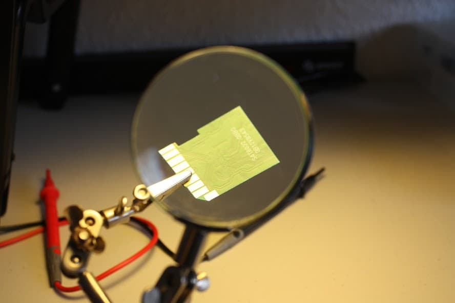
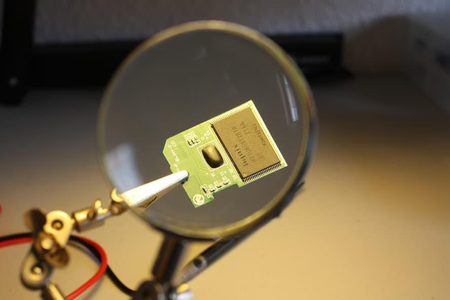
    So, I have collected the image of internal of SD card which was uploaded by Guillermo Amaral.
    Here's few :

    1

    3

    11

    Well most people knows, it uses Nand flash gates, but why Nand gates only ? Why nor Ex-or or anyother ?
    Have you wondered how does a small fabricated plastic containing a very minute chip is capable of storing data upto 32GB ? I don't !

    So, let's discuss how the SD Card works & Share any information you have about SD cards.
    Let's bring back the old-school "Technical debate" back, starting from this discussion.
    0
    Replies
Howdy guest!
Dear guest, you must be logged-in to participate on CrazyEngineers. We would love to have you as a member of our community. Consider creating an account or login.
Replies
  • Apurwa.Thakur

    MemberJul 15, 2013

    Nand gate is logic device which produce output false when all the input are true and its function is use in flash memory.

    Sd card is non-volatile memory use to store digital information.hence nand/nor gate is use in flash memory which contain floating gate transistor to store information.

    I think these gates are only to provide channel for the electron to flow from source to drain in flash memory.(not sure)👎
    Are you sure? This action cannot be undone.
    Cancel
  • Anoop Kumar

    MemberJul 15, 2013

    Abhishek Rawal
    Well most people knows, it uses Nand flash gates, but why Nand gates only ? Why nor Ex-or or anyother ?
    There are two types of memory NAND and NOR and both are universal gate, right😀

    Here is from wiki:
    <a href="https://en.wikipedia.org/wiki/Flash_memory" target="_blank" rel="nofollow noopener noreferrer">Flash memory - Wikipedia</a><a href="https://en.wikipedia.org/wiki/Flash_memory" target="_blank" rel="nofollow noopener noreferrer">Flash memory - Wikipedia</a>
    We know that files are stored in block format which are linked together.that's why NAND while in case of NOR memory data are stored in byte format which needs to be read independently.
    If you format the drive you have option to set block size of 16/32/64 byte allocation which is much bigger than NOR type size (1byte) and easy to store and read data.


    Above is my observation😁, correct me if you find any reliable source☕
    Are you sure? This action cannot be undone.
    Cancel
  • arunchary

    MemberJul 15, 2013

    Two flash-memory technologies in popular use are NOR and NAND.
    NOR flash is suited for storing program code,
    where the CPU wants fast read access but rarely writes to the
    memory. NOR flash has fast read times but slow erase and write times. NOR flas
    h has low density, so large amounts of storage may require mu
    ltiple chips. To access NOR flash, a CPU uses the same data and address lines used to access other parallel memory chips.
    Storage devices use NAND flash, which has fast erase and write times.
    NAND flash also has lower power consumption and is much cheaper than
    NOR flash. A CPU accesses NAND flash chips via data lines and command
    and address registers. NAND flash has high density, so large amounts of
    memory can fit in a small package.The advantages of NAND flash are so
    attractive that some devices use NAND flash for program memory along
    with a RAM cache to improve performance
    Are you sure? This action cannot be undone.
    Cancel
  • arunchary

    MemberJul 15, 2013

    Three varieties of NAND flash are Old Single-level Cell (SLC), New SLC,
    and Multi-level Cell (MLC). MLC memory stores multiple bits in each cell
    and is popular because it’s cheaper to manufacture. However, compared to
    SLC memory, MLC memory supports fewer erase cycles, has slower write
    times, and consumes more power. These are the typical number of erase
    cycles supported by each memory type: Old SLC: 1,000,000, New SLC:
    100,000, MLC: 10,000
    Are you sure? This action cannot be undone.
    Cancel
  • arunchary

    MemberJul 15, 2013

    In general we have Two flash-memory technologies in popular use are NOR and NAND. NOR flash is suited for storing program code,where the CPU wants fast read access but rarely writes to the memory. NOR flash has fast read times but slow erase and write times. NOR flash has low density,so large amounts of storage may require multiple chips. To access NOR flash, a CPU uses the same data and address lines used to access other parallel memory chips. Storage devices use NAND flash, which has fast erase and write times.
    NAND flash also has lower power consumption and is much cheaper than NOR flash. A CPU accesses NAND flash chips via data lines and command and address registers. NAND flash has high density, so large amounts of memory can fit in a small package.
    The advantages of NAND flash are so attractive that some devices use NAND flash for program memory along with a RAM cache to improve performance.
    Three varieties of NAND flash are Old Single-level Cell (SLC), New SLC, and Multi-level Cell (MLC). MLC memory stores multiple bits in each cell and is popular because it’s cheaper to manufacture. However, compared to SLC memory, MLC memory supports fewer erase cycles, has slower write times, and consumes more power. These are the typical number of erase cycles supported by each memory type: Old SLC: 1,000,000, New SLC: 100,000, MLC: 10,000
    Are you sure? This action cannot be undone.
    Cancel
Home Channels Search Login Register