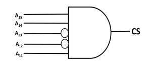
The chip select logic for a certain DRAM chip in a memory system design is shown below.

Mohit Patil

Mohit Patil

@mohit-n7d2qt Oct 26, 2024

Assume that the memory system has 16 address lines denoted by A15 to A0. What is the range of address (in hexadecimal) of the memory system that can get enabled by the chip select (CS) signal?

bNS6-Screenshot%202019-03-31%20at%204.34.31%20PM.png

  1. C800 to CFFF
  2. CA00 to CAFF
  3. C800 to C8FF
  4. DA00 to DFFF

Replies

Welcome, guest

Join CrazyEngineers to reply, ask questions, and participate in conversations.

CrazyEngineers powered by Jatra Community Platform

  • Ankita Katdare

    Ankita Katdare

    @abrakadabra Apr 1, 2019

    A15 A14 A13 A12 A11 A10 A9 ... .... A0
    1    1   0   0   1   0   0 ... .... 0  = C800
    |-Chip select (CS)-| ...   ... .... 1  = C801
    1    1   0   0   1   ...   ... .... .  = ...
    1    1   0   0   1   1   1 ... .... 1  = CFFF 

    Looks Like Option A is the correct answer.