
Novel Devices To Bring Faster Computing - Northeastern University Research
@abrakadabra
•
Oct 23, 2024
Oct 23, 2024
1.4K
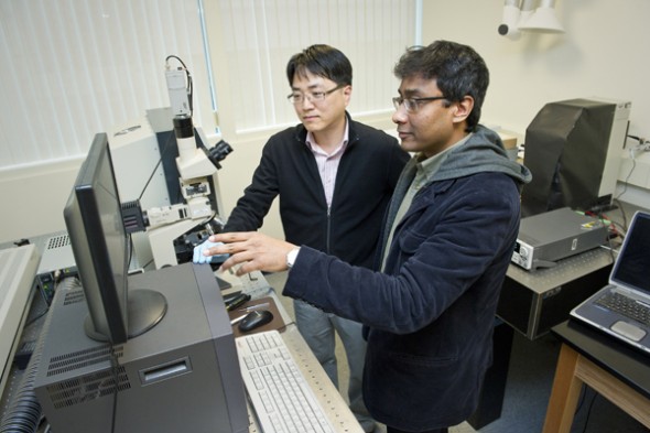
Improving the speed of computing has been a challenging task taken up by researchers all over the worlds. A duo from Northeastern University has developed a series of devices that make every single computational step, out of the billions used for the tiniest tasks on our computers, more efficient and makes the entire computing process way faster. The idea behind this research came from the thought that - if we save time in nanoseconds for every small process in computers, we can have much more faster processing in computers. Swastik Kar, an assistant professor of physics from Northeastern University, who specializes in Graphene-based research started working on this project with Yung Joon Jung, an associate professor in the Department of Mechanical and Industrial Engineering, who specializes in mechanics of carbon nanotubes.
The team used their individual expertise for discovering a physical phenomenon that can form a foundation for highly efficient electronics. They have found that, by replacing the metal with carbon nanotubes in traditional photodiode devices, "light-induced electrical currents" rise much more sharply. This makes way for having newly designed devices that can be turned on and off using light. Since computations are nothing but a series of on-off switches at its core, these findings can help us perform more efficient computations. It is a common belief that the best computers should feature processing using electrical signals and the signal transfer using optical technology.
Interestingly, the devices developed by Kar and Jung are the first ones to integrate electronic and optical properties on a single electronic chip. By collaborating with a team with Young-Kyun Kwon, a professor from Kyung Hee University, in Seoul, Korea, the computational modeling for this project was carried out. The three devices that the team has developed include an AND Gate and OR Gate. The AND-gate takes both an electronic and an optical input to generate an output. Whereas, the OR gate can generate an output if either of two optical sensors is engaged.
The third device, consisting of 250,000 miniature devices assembled over a centimeter-by-centimeter surface, works just like the front-end of a camera sensor. More integration work is need on this device to make it fully viable. With their novel techniques, they have been able to develop much more scalable electronics devices. Their research work is now published in the journal Nature Photonics.
What are your thoughts on that? Share with us in comments below.
Source: #-Link-Snipped-#