
How does the transistor work?
How does the transistor work?
P.S. :We are dealing with normal operation of the transistor for this expalnation
1. The process of applying dc voltages across different terminals of the transistor is called as biasing.
2. For normal operation of the transistor the emitter base junction is forward biased and the collector base junction is reverse biased.
3. The depletion region width at the emitter base junction is small will it is large at the collector base junction because of doping concentration.
4. Thus the effective base width Wb between the two depletion regions is very narrow.
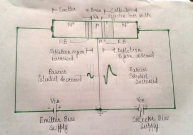
5. Electrons are injected into the emitter region by the emitter base supply VEB . this electrons have enough energy to overcome the barrier potential .
6. These electrons then enter the thin, lightly doped base region. Only a few electrons recombine with the holes in the base region.
7. Thus the concentration of the electrons on the emitter side is very large and that of the collector side is so very small and the gradient of electrons concentration in the base is very large.
8. Now these electrons diffuse into the collector region because of small thickness of the base region.
9. Collector is reverse biased and creates a strong electrostatic field between base and collector.
10. This field immediately collects the diffused electrons.
11. Only about 1 to 5 percent of electrons recombine with holes in the base region. Remaining 99 to 95 percent of electrons are collected by the collector electrode.
12. Thus the emitter current is equal to the sum of base current and the collector current.
IE=IB+IC
13. The ratio of the collector current IC to the emitter current IE is called as α and is called as the current amplification factor. It cannot be higher than unity.