CrazyEngineers
  • Inmos


    cmos
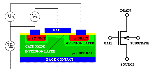
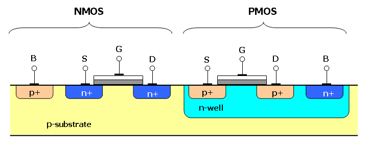
    I found these two diagrams Now my doubt is that in the first NMOS diagram the p-substrate is directly taken as base but in the second CMOS diagram p+ is taken as base what might be the reason for that?
    Replies
Howdy guest!
Dear guest, you must be logged-in to participate on CrazyEngineers. We would love to have you as a member of our community. Consider creating an account or login.
Replies
  • Jeffrey Arulraj

    MemberJul 29, 2015

    If you have seen any package of MOSFET you will note that there are 4 lets from them and even your academics will tell there is a pin called substrate.

    In the second image we have P layer as a substrate and the P+ serves as the Body of the MOS and the p layer has insufficient dopant concentration to provide charge carriers to enable conduction in the Transistor

    Where as in the case of a individual NMOS there is no need for two P layers as you know that the amount of carriers got is more than enough to turn the device on

    Feel free to ask any question related to this.
    Are you sure? This action cannot be undone.
    Cancel
  • DivyaSep

    MemberJul 29, 2015

    Jeffrey Samuel
    If you have seen any package of MOSFET you will note that there are 4 lets from them and even your academics will tell there is a pin called substrate.

    In the second image we have P layer as a substrate and the P+ serves as the Body of the MOS and the p layer has insufficient dopant concentration to provide charge carriers to enable conduction in the Transistor

    Where as in the case of a individual NMOS there is no need for two P layers as you know that the amount of carriers got is more than enough to turn the device on

    Feel free to ask any question related to this.

    Thank you so much
    Are you sure? This action cannot be undone.
    Cancel
Home Channels Search Login Register