Semiconductor Device:P-N Junction Diode
P-N Junction Diode
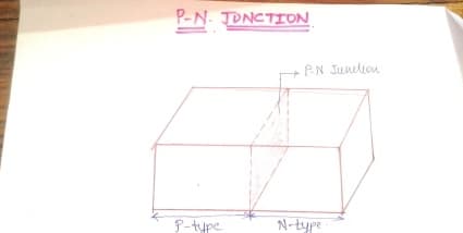
1. P-N junction is produced by placing a layer of p-type on one side and n-type on the other.
2. It act as the control element for the performance of many of the semiconductors devices such as rectifiers, amplifiers, switching devices, linear and integrated devices.
3. Now p-type has mobile holes accept and negative acceptor ions which are fixed, while n-type has mobile electrons and same number of fixed donor positive ions.
4. Each region is electrically neutral because each of them consists of equal number of positive and negative charge carriers.
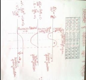
5. On to the formation of the junction, some free holes from p-side diffuse (get into) into n-side and some free electrons from n-side diffuse into p-side.this is because of the concentration of electrons is higher in one side and that
of the holes is higher on p-side called as density gradient. This process is called as diffusion.
6. Because of the diffusion of the charges the electric field gets generated across the junction. The electric charges stay near the junction and consist of immobile ions.
7. Thus because of the diffusion , negative potential is build up across p-side and positive potential is build across n-side. This prevents further migration of holes and electrons from both sides. Thus it creates barrier potential at the junction.
8. The region across the junction is completely ionized. It is called as space charge region, transition region or depletion region.
1. P-N junction is produced by placing a layer of p-type on one side and n-type on the other.
2. It act as the control element for the performance of many of the semiconductors devices such as rectifiers, amplifiers, switching devices, linear and integrated devices.
3. Now p-type has mobile holes accept and negative acceptor ions which are fixed, while n-type has mobile electrons and same number of fixed donor positive ions.
4. Each region is electrically neutral because each of them consists of equal number of positive and negative charge carriers.
5. On to the formation of the junction, some free holes from p-side diffuse (get into) into n-side and some free electrons from n-side diffuse into p-side.this is because of the concentration of electrons is higher in one side and that
of the holes is higher on p-side called as density gradient. This process is called as diffusion.
6. Because of the diffusion of the charges the electric field gets generated across the junction. The electric charges stay near the junction and consist of immobile ions.
7. Thus because of the diffusion , negative potential is build up across p-side and positive potential is build across n-side. This prevents further migration of holes and electrons from both sides. Thus it creates barrier potential at the junction.
8. The region across the junction is completely ionized. It is called as space charge region, transition region or depletion region.
0