What is the use of RC ladder in fsk demodulator using PLL?
![[IMG]](proxy.php?image=http%3A%2F%2Fwww.circuitstoday.com%2Fwp-content%2Fuploads%2F2009%2F09%2Fne-se-565-as-fsk-demodulator.jpg&hash=d62bbda79fca7daa3103bc3da4a5ea8f)
can any one please explain the use of RC ladder in above circuit...?
0
Member • Jul 30, 2014

Administrator • Jul 30, 2014
Member • Aug 1, 2014
Member • Aug 1, 2014
Member • Aug 2, 2014
![[IMG]](proxy.php?image=http%3A%2F%2Fwww.circuitstoday.com%2Fwp-content%2Fuploads%2F2009%2F09%2FNE-SE-PLL-Block-Diagram.jpg&hash=8a69ad825b0facc61fd99a2a64007fd2)
Member • Aug 2, 2014
SmiechHi,
I think the three-stage RC ladder filter is employed for removing the sum frequency component from the output. The VCO frequency is adjusted with R1 so that the dc voltage level at the output (pin 7) is the same as that at pin 6. An input at frecuency 1,070 Hz drives the demodulator output voltage to a more positive voltage level, driving the digital output to the high level (space or + 14 V). An input at 1,270 Hz correspondingly drives the 565 dc dc output less positive with the digital output, which then drops to the low level (mark or -5V).
Member • Aug 2, 2014
Member • Aug 2, 2014
Member • Aug 2, 2014
Member • Aug 4, 2014
Member • Aug 4, 2014
thank you for your kind reply sir...Smiech
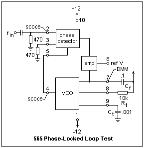
The 565 is a bipolar chip that contains a phase detector and a VCO. These modules are not completely separate, as they are in the 4046, so they are a little more difficult to experiment with individually. The input to the 565 is intended to be a sine wave, or something similar, so the phase detector is designed accordingly. It is a double-balanced modulator, and does for analog signals essentially what the XOR gate does for square waves. It is a Type I phase detector, with a range of 0 to 180° in phase. The circuit is shown at the left. The inputs at pins 2 and 3 of the 565 are directly to the bases of the input transistors. The square wave from the VCO switches the transistors that are conducting at any moment, and the outputs are taken differentially from the collectors. There is a minimum output for zero phase difference, and a maximum for antiphase. The output is sent through amplifying circuits directly to the VCO, whose DC input appears at pin 7. This is from 8 to 10 V, so a reference voltage is output at pin 6 to make connection with op-amps easier.