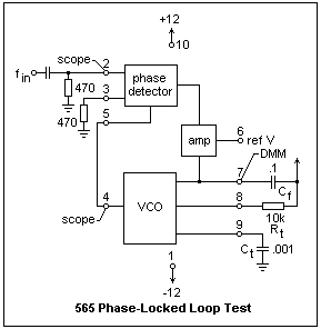
Replies
Welcome, guest
Join CrazyEngineers to reply, ask questions, and participate in conversations.
CrazyEngineers powered by Jatra Community Platform
-
@joy-8GOU7k • Jul 30, 2014
could any one please help me to understand the use of 3 stage RC filter at the output of PLL? -
@abrakadabra • Jul 30, 2014
Tagging #-Link-Snipped-# #-Link-Snipped-# #-Link-Snipped-# -
@joy-8GOU7k • Aug 1, 2014
thank you mam..for your reply..
but how should i use those taggings.... -
@smiech-IwJ5fO • Aug 1, 2014
Hi,
I think the three-stage RC ladder filter is employed for removing the sum frequency component from the output. The VCO frequency is adjusted with R1 so that the dc voltage level at the output (pin 7) is the same as that at pin 6. An input at frecuency 1,070 Hz drives the demodulator output voltage to a more positive voltage level, driving the digital output to the high level (space or + 14 V). An input at 1,270 Hz correspondingly drives the 565 dc dc output less positive with the digital output, which then drops to the low level (mark or -5V). -
@joy-8GOU7k • Aug 2, 2014
thank you sir....but could you please explain me then what is the purpose of the low pass filter in the pll block...? -
@joy-8GOU7k • Aug 2, 2014
SmiechHi,
I think the three-stage RC ladder filter is employed for removing the sum frequency component from the output. The VCO frequency is adjusted with R1 so that the dc voltage level at the output (pin 7) is the same as that at pin 6. An input at frecuency 1,070 Hz drives the demodulator output voltage to a more positive voltage level, driving the digital output to the high level (space or + 14 V). An input at 1,270 Hz correspondingly drives the 565 dc dc output less positive with the digital output, which then drops to the low level (mark or -5V).![[IMG]](proxy.php?image=http%3A%2F%2Fwww.circuitstoday.com%2Fwp-content%2Fuploads%2F2009%2F09%2FNE-SE-PLL-Block-Diagram.jpg&hash=8a69ad825b0facc61fd99a2a64007fd2)
thank you sir...then what could be the use of low pass filter arrangement in the pll block...? -
@smiech-IwJ5fO • Aug 2, 2014
The low pass filter helps keep the VCO from hunting. The filter supplies the control voltage to the VCO, and it helps insure the voltage is reasonably clean DC. Otherwise, you can imagine that an unfiltered control input could cause the PLL to become an oscillator, with the VCO always chasing the signal frequency, but constantly under-and overshooting the stable point. It also places an upper limit on the PLL's response, so you don't get it trying to lock on radar frequencies. -
@smiech-IwJ5fO • Aug 2, 2014
The Phase-Locked Loop (PLL) is a device with many interesting applications including frecuency synthesis, FM demodulation, and TV sweep circuits. Its operation seems nearly miraculous, but feedback makes the job easy, and it is an excellent example of feedback in action.
PLL, despite their importance and interest, are usually not treated in university electronics course, though they are very much electronics and help the understanding gratly.
Once its operation is understood, all the applications will follow easily. We generally think of the circuit as accepting an input at some frequency and providing an output at the same frequency that is not a copy of the input, but the output of an independent oscillator whose frequency is controlled by feedback. The output of the oscillator is compared to the input, and if the frequencies are different, the frequency of the oscillator is altered to reduce the difference.
This is what it looks like, but it is better to consider the controlled quantity to be the phase of the signals. A signal of frequency f Hz changes phase by 2πf radians per second. In general, the phase in radians is 2π times the integral of the frequency with respect to time. The phase-locked loop compares the phases of the input signal and the oscillator signal, and adjusts the oscillator to reduce the phase difference. -
@smiech-IwJ5fO • Aug 2, 2014
The 565 is a bipolar chip that contains a phase detector and a VCO. These modules are not completely separate, as they are in the 4046, so they are a little more difficult to experiment with individually. The input to the 565 is intended to be a sine wave, or something similar, so the phase detector is designed accordingly. It is a double-balanced modulator, and does for analog signals essentially what the XOR gate does for square waves. It is a Type I phase detector, with a range of 0 to 180° in phase. The circuit is shown at the left. The inputs at pins 2 and 3 of the 565 are directly to the bases of the input transistors. The square wave from the VCO switches the transistors that are conducting at any moment, and the outputs are taken differentially from the collectors. There is a minimum output for zero phase difference, and a maximum for antiphase. The output is sent through amplifying circuits directly to the VCO, whose DC input appears at pin 7. This is from 8 to 10 V, so a reference voltage is output at pin 6 to make connection with op-amps easier. -
@joy-8GOU7k • Aug 4, 2014
thank you for your kind reply sir... -
@joy-8GOU7k • Aug 4, 2014
thank you for your kind reply sir...Smiech
The 565 is a bipolar chip that contains a phase detector and a VCO. These modules are not completely separate, as they are in the 4046, so they are a little more difficult to experiment with individually. The input to the 565 is intended to be a sine wave, or something similar, so the phase detector is designed accordingly. It is a double-balanced modulator, and does for analog signals essentially what the XOR gate does for square waves. It is a Type I phase detector, with a range of 0 to 180° in phase. The circuit is shown at the left. The inputs at pins 2 and 3 of the 565 are directly to the bases of the input transistors. The square wave from the VCO switches the transistors that are conducting at any moment, and the outputs are taken differentially from the collectors. There is a minimum output for zero phase difference, and a maximum for antiphase. The output is sent through amplifying circuits directly to the VCO, whose DC input appears at pin 7. This is from 8 to 10 V, so a reference voltage is output at pin 6 to make connection with op-amps easier.