Characteristics of P-N Junction diode
Characteristics of the PN junction diode
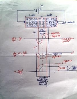
Forward Biased:
1. When the external electrical field is connected such that the positive terminal of the battery is connected to p-type and negative terminal is connected to n-type, then the junction is said to be forward biased.
2. In this arrangement, the holes from the p-side are repelled from the terminal and are attracted towards the junction. Similarly the electrons ae repelled from the negative biased and are attracted towards junction.
3. Thus the depletion region gets reduced.
4. Barrier potential also gets reduced. If the applied potential is increased further the barrier potential further reduces and charge carriers can easily flow through it.
5. Thus the majority current flows.
6. Once the barrier potential (0.3V for Ge and 0.7 for Si) is removed, junction resistance becomes almost zero and low resistance path is established, thus the current called forward current flows through to the circuit.
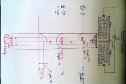
Reverse Biased:
1. If the external electric field is connected such that positive terminal is connected to n-side and negative terminal is connected to p-side then the junction is said to be reversed biased.
2. Thus electrons from n-side are attracted to positive bias terminal and holes from p-side are attracted to negative terminal.
3. Because of this the depletion region widens. The barrier potential gets increased by the amount by which the bias is applied. Thus a large amount of resistance is build up.
4. Thus only a small amount of current called as reverse current or leakage current flows through the device.