
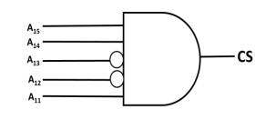
The chip select logic for a certain DRAM chip in a memory system design is shown below.
Assume that the memory system has 16 address lines denoted by A15 to A0. What is the range of address (in hexadecimal) of the memory system that can get enabled by the chip select (CS) signal?
- C800 to CFFF
- CA00 to CAFF
- C800 to C8FF
- DA00 to DFFF
Replies
-
 Ankita Katdare
A15 A14 A13 A12 A11 A10 A9 ... .... A0
1    1   0   0   1   0   0 ... .... 0  = C800
|-Chip select (CS)-| ...   ... .... 1  = C801
1    1   0   0   1   ...   ... .... .  = ...
1    1   0   0   1   1   1 ... .... 1  = CFFF
Looks Like Option A is the correct answer.
You are reading an archived discussion.
Related Posts
I need help to identify a graduate project in GIS
This instructable describes how to build a neck-through electric bass guitar with only a minimal number of electric tools.https://www.instructables.com/id/Neck-Through-Bass-Guitar/?utm_source=newsletter&utm_medium=email
As there are lot of people paying attention towards insurance of life insurance of car insurance of travel and much more...is it possible to give insurance to electronic appliances such...
We are new Start-up to built parking solutions and there are huge opportunities in this field at apartments, smart cities and commercial parking... But since we are new start-up we...
ANYONE WHO HAS DONE ENGINEERING DOESNT MAKE HIM AN ENGINEER.. In India "engineering" has been a trend.. people have made it as shortcut to get a govt job and settle...