-
Muffy
Member •
Sep 2, 2009
Hi
This is a really interesting project. I'm going through the links , and ill try to answer your questions.
:smile:
Are you sure? This action cannot be undone.
-
Hi there muffy. I really appreciate you taking your time to go through this. You truly are god send. Will post my questions for you tomorrow as soon as i have them already. Thank you so much for your time.
Are you sure? This action cannot be undone.
-
Hi there Muffy.....
So here are my questions:
Regarding both documents:
1. Zero crossing detector section:
a.It says that the RBO pin of the pic will be changed from Vss-0.6V. Is this a set value due to the diodes or is there a way of calculating this value?
b.Input threshold will be 0.8Vdd or o.2Vdd. Why? Where do you get the values 0.8 and 0.2 from?
2.What modifications would you make on all these circuits for an Ac of 230v at 50Hz. Especially diagrams 3 of 5 and 5 of 5 from the AN236 document.
3.Please explain how diagram 4 of 5 functions.
4.Diagram 5 of 5: How would you modify it for 230V @50Hz. Please explain this circuit to me. Also power in refers to the the AC input to the the transmitter and receiver respectively. But what is the POWER OUT point?? What is it used for?
5.You would obviously require two different power supplies, right? Because both the transmitter and receiver need to be connected over the AC lines for communication.
Regarding the second document –not AN236!!!!!
1. Can you make out what type of LCD display is used here?
2. Look at figure 1 under the receiver section:
a. The Ac mains are connected directly to the voltage limiter. How?
b. There are pins on the PIC microcontroller that are connected to relays. Why???
3. SOFTWARE SECTION
a. Algorithm for transmitter: STEP 3 says to configure RB1-RB4 as input ports – this would be for the switches, right?
BUT
The Algorith for the receiver: STEP 1: sets RBO-RB4 as output-why???
Are they using two separate PICS for this project??
b. LOOK at the Flow Charts: On all the flow charts there is a circle with an R in it.
What is this????
Thanks a lot for all the help....really really appreciate it
![[IMG]](proxy.php?image=http%3A%2F%2Fwww.electro-tech-online.com%2Fimages%2Fsmilies%2Fsmile.gif&hash=25920eebec654f37825f2d7c3d490bea)
Are you sure? This action cannot be undone.
-
Muffy
Member •
Sep 3, 2009
Whoa! Loaded questions. Ill compile my answers and get back to you in a while.
😀
Are you sure? This action cannot be undone.
-
Muffy
Member •
Sep 3, 2009
Hi
I have tried to answer your queries as accurately as possible but i might have made a few boo boos .😔
To address your questions in the first document
1)
a)
The RB0 pin has an internal clamping circuit to prevent to voltages at the pin from going below Vss (0V) and above +5.5V and damaging the pin.So During the negative half cycle of the AC Voltage the input at the pin is clamped to Vss -0.6 V (which is -0.6V because Vss is 0v) . The -0.6V is because of the voltage drop across the diode , and this small voltage is acceptable. This voltage is constant , no calculation is necessary and dose not affect the performance of the circuit in anyway.
b)
The RB0 pin is a Schmitt trigger buffer , which means its designed to operate so that-
The input reads a logic High ( logic 1) if the input voltage exceeds 0.8Vdd. which would be normally 4V if your supply voltage is 5V.
The input reads a logic Low ( logic 0) if the input goes below 0.2Vdd which would be 1V if your supply voltage is 1V
This is internally achieved by the controller to avoid false logic in case of noise. You need not be concerned about this.
2)
The only modification necessary is that the value of VDR (page5/5), currently rated at 130V must be increased to 240V. The rest of the components will survive the increased voltages quite comfortably.
3) Diagram 4/5
i) The XIOCIRCUITS label (Input from the AC receptacle ) in series with the 5mohm resistor and ZEROX label (to pin RB0), samples the AC voltage and sets the interrupt when a 0V is detected.
ii) The XIOCIRCUITS label in series with the High pass filter circuit (the reisistor and capacitor in parallel) and the two zener diodes and the CARRIERDATA label are part of the reciever circuit( the part which decodes the 120khz carrier frequency to read a logic 1)
iii) The XOUT label (output from the PWM of microcontroller), and transistor circuit (which is nothing but a driver circuit which allows a higher current to be drawn without effecting the microcontroller pin) in series with the filter circuit connected to the XIOCIRCUITS label , is the transmitter circuit (The circuit which sends a 120khz carrier frequency on the power line).
4) Okay , lets reffer the "transmitter" as the controller module and the "reciever" as the application module.
The controller module needs only the Power in, which is the wall receptacle its connected to.Because its sole operation is sending and receiving command over the power line. No appliance like a light bulb is going to be connected to it.
In contrast the appliance module needs a power in and power out ( a plug that connects into the wall and a socket so that an appliances plug may be connected to it). The power in is connected to control circuitry to read and send signals. It is also connected to another 3 socket receptacle so that a lamp or appliance may be connected to it. The input is not directly connected to the output, but via a TRIAC (Q1). The Triac controls the passage of AC current through it. The triac is in turn controlled by the microcontroller. Thus the output can be switched on or off or dimmed( by assigning different triggering angles to the triac)
As for the working
i) The TRIAC label in series with ||R11 and diode simple control how much power form input wall receptacle should be transferred to output socket. It can be switched on or off or partially on.
ii) The rest of the circuit is the transformerless power supply circuit which extracts power from the AC supply and converts in into DC 5 V supply to power the microcontroller ,the LCD display and remaining circuits.
5)
There are two modules required
i) The controller module- It consists of transformerless power supply, transmitter circuit, receiver circuit , zero detector circuit, LCD display circuit and switches. This circuit plugs in to one of the wall receptacles and is used for controlling the other modules
ii) The application module- This is the module that is controlled by the controller module, it is attached to another wall receptacle and may be connected to a lamp or fan or any other appliance. This circuit consists of the transmitter circuit, receiver circuit, zero detector circuit, load cell (triac circuit) and or the LDR (CdS) circuit.
Refrain from referring to them as transmitter or receiver circuits because both modules perform both operations.
Now coming to the second document
1)
The LCD display is a HD44780 based display. Its a standard parallel type display with 14 to 16 pins and is widely available in the market, you shouldn't have any problems acquiring one if need be.
2)
a) If you notice , there is a high pass filter circuit between the source and voltage limiter. The high pass circuit is designed to filter out voltages at frequencies below 32Khz. So the AC voltage at 50Hz has no chance getting through it. 😁
b) 😒 Ehm? I don't see any pins connected to any relays, the circuit has none. Can you please specify which pins so i can clarify?
3)
a) In the controller module:-
The RB0 is the interrupt pin and so it should be configured as an input. The RB1-RB5 pins are connected to the switches and must be obviously configured as inputs.
In the application module:-
Again, the RB0 should be configured as an input, there is a typo in the document , RB0 is always an input. The rest of the pins RB1-RB5 can be configured as inputs or outputs and left unconnected , it matters not.
b)
In a flowchart A circle containing a letter or number means that this chart connects to another chart on a different page. The same circle and number are then the entry point on the new page.
On page 26 of the document there is a circled R with an arrow pointing towards the flowchart. This indicates that all the other circled R on the other pages connect to the R on page 26.
Sorry for the long drawn answers, hope they help. Let me know if you need any further clarifications.
Good luck
😁
Are you sure? This action cannot be undone.
-
Oh my gosh! This is amazing. Thank you so much for being so prompt. You really are a star😀 i am going to take a look at these answers and let you know if i need some more help and clarification. I really appreciate this.
Are you sure? This action cannot be undone.
-
@ Muffy: Awesome! Great going! 😀 Keep it up!
Are you sure? This action cannot be undone.
-
Muffy
Member •
Sep 4, 2009
Thanks! Happy to help.😀 .
@preeste: ARGH! I have blundered. In q 4) you have asked for an explanation of sheet 5/5 , i have detailed the explanation of 3/5. And in answer 2) the VDR isn't in 5/5 but in 3/5.
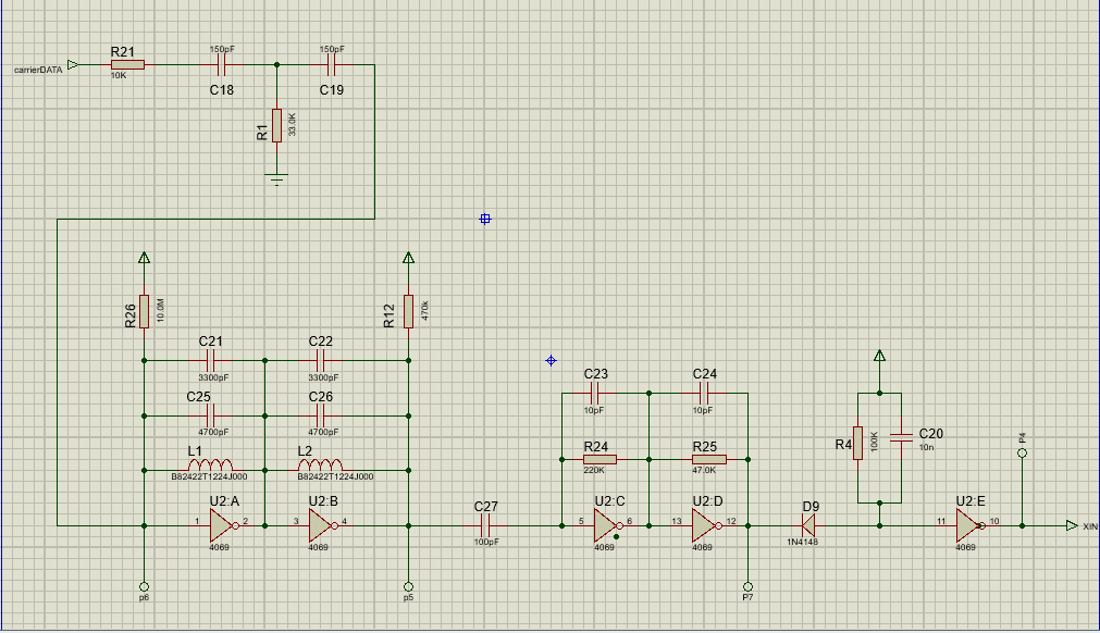
The circuit on sheet 5/5 is the part which receives and decodes the 120khz carrier frequency to logic 1. It actually begins on sheet 4/5 with the XIOCIRCUITS label , high pass filter, voltage limiter and CARRIERDATA label. It then continues to page 5/5 , where there is yet again another high pass filter which filters out any low frequency voltages , then a tuned amplifier, which amplifies signals of only a particular frequency, in this case 120Khz. The next stage is an untuned amplifier which further increases the magnitude of the signal. The next stage is an envelope detector.
"An envelope detector is an electronic circuit that takes a high-frequency signal as input, and provides an output which is the "envelope" of the original signal." [From Wikipedia]
If you were to feed the amplified 120khz carrier wave into the microcontroller , the controller would read a number of impulses (101010101), which would be disastrous, so we need a circuit that would even out the voltage and give a single voltage when a 120khz signal is present. This is achieved by the envelop detector. Its like marking a dot at the peak of every cycle and connecting the dots, you would get a straight line, constant voltage, perceived by the microcontroller as logic 1. TADA!
To account for higher supply voltage, capacitors C17, C14 and C15 rated voltages have to be greater than 400 . The zener diode ,D6, should be rated for 5W.
😁
Are you sure? This action cannot be undone.
-
Hi there Muffy....sorry for the time off...was just trying to take in everything you said and make sense out of it......but now i have even more questions.
This are questions based on the Microchip application note:
1. Refering to diagram 3/5:
a. What is meant by the scope adapter circuit? What does it do? How does it function?
b. How would you go about designing this circuit from scratch ie the steps you would take, the formulaes you would use, how you would determine what components to use and component values etc
2. Diagram 4 of 5
a. Why are the controller module and the application module circuitry designed together on one circuit?
b. Are the X-10 circuits label and the highpass filter not in parallel?
c. Can you explain this circuit in more detail.If you had to design it from scratch how would you go about it...i mean the steps you would take, the formulaes you would use, how you would determine what components to use and component values etc etc.
d. What is the point of the two diodes and how do you choose the 6.8V diodes. And why are they connected the way they are (cathode to cathode)?
e. How do you determine the values of the resisors R20 and R19? Are they 200 and 50 ohms respectively?
e. Why is that particular transistor choosen.
3. Referring to diagrams 3,4,5
Would you please mind showing me how to design these circuits from scratch. How do you start, what do you look at, what formulaes to use where, how do you determine what component to use, how to find the correct component vales etc etc.
This would be very helpful. It will give me a much better understanding of this application......i am sorry about this...its just that my electronics is terrible.
REFERRING TO THE OTHER DOCUMENT!!!!
HARDWARE
1. In my first post of questions i had asked the following question to which you said you did not understand which diagram i was referring to. "There are pins on the PIC microcontroller that are connected to relays. Why???"
This question refers to the circuit on page 22. Look at the PIC right below the RBO pin. There are three pins that go to relays. Where and what is this for?
2.Does this document use a TRIAC? If not how would you modify diagram 3 of 5 accordingly?
3. This application only uses 4 switches instead of 5, right? According to page 5 under the transmitter section there are said to be used for the following functions respecively: select house code, device, function code and sending the data through the powerline. How is this done?
SOFTWARE:
Can you please take a look at the code and answer these questions for me:
1. Does the code as it is given in this document function and work fully?
2.Would you please maybe comment each line of the code for me so that i can understand it better.
Thank you so very very much for your help.....i know this is really loaded but i would appreciate all the help i can get. Thank you in advance. looking forward to hearing from you.
Regards
Preeste
Are you sure? This action cannot be undone.
-
By the way, in your last post you mention at the bottom that to account for higher supply voltage, capacitors C17, C14 and C15 rated voltages have to be greater than 400. Was this refering to diagram 3 of 5? And if so did you mean C16 instead of C17 because i cant find C17? And it must be greater that 400 what? As in what is the unit? How do you find all this?
Are you sure? This action cannot be undone.
-
hey there MUFFY....here are a few more questions....the more i look at this document the more questions i have.
these are all based on schematic 5 in appendix c of the an236 application document.
Refering to schematic 5 in appendix C, i have the following questions?
1. How does one go about designing this circuit ie what are the formulaes that are used, how do you know where to place each component, how do you determine the values of the various components.
2. the circuits labelled tuned amplifier and untuned amplifier, are they really amplifier circuits. Should amplifier circuits not contain either transistors or operational amplifiers? Are they not some sort of high pass filter?
3.I know what the basic purpose of the amplifiers are for but how do they actually function? What are each of the components used for?
4. what does the envelope detector do? What do each of the components do?.
5. What is the purpose of the 5 not gates in this circuit?
6. What are the functions of the following components: C19,R21,C27,D9?
7. what would the signal waves look at at these various points of this circuit: at the input or carrierdata, after the high pass filter, after the tuned amp, after C27, after the untuned amp, after D9, after the envelope detector but before U2:E and after U2:E
8. Could you try simulating these circuits on some program like Powersim.....are the waveforms what u expect it to be? please explain if u can?
thank you so so very much.....i am so sorry to rush you but this is really urgent now....hopefully i hear from u very very soon😀
Thank you so much Muffy...you are truly god sent.
Are you sure? This action cannot be undone.
-
Muffy
Member •
Sep 11, 2009
1a) Scope Adapter circuit
This is an optional circuit. It lets you attach an oscilloscope to the circuit.(Oscilloscopes are used to observe the wave shape of an electrical signal) There are 2 channels, you can observe the supply voltage on one channel and on the other channel you can observe the 120khz carrier frequency. Resistors R13 and R15 reduce the voltage of supply , to be sampled by the oscilloscope. The capacitor C13 and resistor R16 allow only the 120khz signal to pass through and reach the oscilloscope.
2a)
You have misunderstood . The control and appliance module are different physical pieces of equipment. You will have to build two individual modules ie. TWO CIRCUITS. One for the controller and another for appliance module. But you dont have to replicate the entire circuit twice. There are certain parts not required by the controller module , and certain components not required by the appliance module.
i) The controller module- It consists of transformerless power supply, transmitter circuit, receiver circuit , zero detector circuit, LCD display circuit and switches.
ii) The appliance module- This circuit consists of the transformerless power supply circuit ,transmitter circuit, receiver circuit, zero detector circuit, load cell (triac circuit) and or the LDR (CdS) circuit.
The circuits in bold are required on both the modules, you will have to build two circuits each containing these and elements and then you can add the display circuit and switch to the control module, the appliance module don't need them , but you will have to include the load cell and ldr circuit in it.
b)
The resistor R17 (5 million ohm) is a very very very high resistance value. While the capacitor C17 appears as a short circuit (almost) at frequency of 120khz , so the entire signal passes through the capacitor and completely avoids the resistor R17 so for all practical purpose the XIOCIRCUITS label is in series with the high pass filter.
Then what business the R17 has there? Well , even if cannot allow current to flow through it , the supply voltage will be accurately represented to the zero detector pin.
c)
You will have to learn about functioning of each component individually before you can appreciate their working in the circuit, there are many websites that can help you with basic electronics.
d)
These diodes are zener diodes(diodes which work as regulators in reverse bias). In this circuit they are used to drop the voltage to a fixed value (6.8V). No matter how high the voltage across them is the output voltage will always be 6.8V. ( #-Link-Snipped-# [link])
In the positive half cycle of the signal, diode D7 limits the voltage , while D8 just acts as a short circuit ( just a piece of wire).
In the neative half cycle of the signal, diode D8 limits the voltage, while D7 acts as a short circuit.
e)
The transistor works as a simple switch here. When the base is supplied with a high voltage (5v) a base current of ((5V-0.7V)/200ohms) is produced.
Where 5v is voltage from XOUT label, the 0.7V the base voltage drop and 200ohms resistor R20.
This saturates the transistor (Switches it on).
R19 is 50Kohm not 50 ohm . The R19 lowers the current through the transistor (5V/50kohm).
The transistor 2n2222 is a very widely used switching transistor, but any other switching transistor can be used.
3)
Don't look at the circuit as a collection of individual components. Identify each functional block of the circuit, then learn how the entire block functions on the whole, don't even look at the schematic diagram , its scary. AN236 has detailed explanation of each block,some with formulas. If formulas aren't provided then the values of those components aren't critical.
The other document
1)
Ahh i see them now! These are optional . Relays are just switces. If you need to switch appliances you could make used of these pins and program the microcontroller with the appropriate software (#-Link-Snipped-# [link])
2)
Nope, this document doesn't have the triac. But not having a triac (or at least a relay) defeats the purpose of the entire thing. The triac or relays are switching devices and the appliance module is meant to switch an appliance on or off, the triac also allows the voltage to be varied, for dimming lights.
You could replace the triac with a relay. In sheet 3/5 you could remove R11 D5 and Q1 and in its place add the relay circuit in this link (#-Link-Snipped-# [link]) the relay pins 4 and 5 connect to the N and N of Power in and Power out.
3) Yes in this particular document there are 4 switches. The switches are directly connected to the microcontroller with a pull up resistor (refer App note). The funcions of the switches are written in the software.
If you want to to implement this project . I advice you to refrain form using this document. Build the circuit from the microchip app note, and write the software yourself. The provided program is incomplete and unreadable.
Good luck.
Are you sure? This action cannot be undone.
-
hey there....thanks a lot for the answers. Can i plese bother you one last time.....this has to do with schematic 5 of 5 in an236. The more i look at it the more confused i get.
Refering to schematic 5 in appendix C, i have the following questions?
1.. the circuits labelled tuned amplifier and untuned amplifier, are they really amplifier circuits. Should amplifier circuits not contain either transistors or operational amplifiers? Are they not some sort of high pass filter?
3.I know what the basic purpose of the amplifiers are for but how do they actually function? What are each of the components used for?
4. what does the envelope detector do? What do each of the components do?.
5. What is the purpose of the 5 not gates in this circuit? ????????????????
6. What are the functions of the following components: C19,R21,C27,D9?
7. what would the signal waves look at at these various points of this circuit: at the input or carrierdata, after the high pass filter, after the tuned amp, after C27, after the untuned amp, after D9, after the envelope detector but before U2:E and after U2:E
8. Could you try simulating these circuits on some program like Powersim.....are the waveforms what u expect it to be? please explain if u can?
thank you so so very much.....i am so sorry to rush you but this is really urgent now....hopefully i hear from u very very soon:smile:
Are you sure? This action cannot be undone.
-
Muffy
Member •
Sep 13, 2009
<a href="https://www.falstad.com/circuit/e-invertamp.html" target="_blank" rel="nofollow noopener noreferrer">Inverter Amplifier</a> This will help understand how not gates,inverters, can amplify.
Are you sure? This action cannot be undone.
-
Hello .Thanks for the post you put up last. I took a look at it and it made sense. But I have more issues now. The CMOS not gates can be used to amplify its input signal by about 150 times when its output is connected to its input via a resistor of about 1M.
Please take a look at the circuit 5 0f 5 again in appendix c. Now the above circuit receives a AC signal modulated with a 120KhZ square wave . Apparently the first stage represents a 120Khz tuned high pass filter with amplification and the next is an un-tuned high pass filter. My understanding of high pass filters is that you have a capacitor in series to a resistor where the capacitor is connected to the signal and the resistor is connected to ground. But this looks nothing like it. On the contrary the “un-tuned filter” actually has a capacitor and a resistor in parallel!!!!!! How does that even create a high pass filter??? Please try and explain how this circuit functions? I am really baffled by it. Point C is the input to the envelope detector…that part makes sense
Are you sure? This action cannot be undone.
-
hello muffy,please can you help me , can you explain to me how diagram 5 of 5 functions.
Are you sure? This action cannot be undone.
-
Nesryne
hello,please who can you help me , toexplain to me how diagram 5 of 5 functions x10 AN236 .

Are you sure? This action cannot be undone.