What is Bipolar junction transistor?
Bipolar Junction transistor:
1. A solid state device made up of single crystal.
2. A current controlled device.
3. It is compact in size, rugged construction, low operating voltage, high efficiency and long life with no ageing effect.
4. Main drawbacks are that it has loud hum noise, restricted operating point and operating frequency.
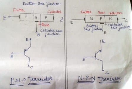
When the N-type of material is sandwiched between two P-type of material then a PNP transistor is formed.
When a P-type of material is sandwiched between two N-type of material then it is said as NPN transistor.
5. Each transistor has two PN junctions. One junction is called emitter base junction because it is the junction between emitter and the base and other is called collector base junction as this junction is between collector and base.
Transistor terminals;
6. There are three part or terminals in the transistor. One side section supplies free charges or emits charges is called as the emitter. The other side section collects these charges called as the collector. The center section is called as the base. Let’s discuss them in detail:
a. Emitter: it is the left hand region of the transistor. Its main function is to supply majority charge carriers to the base. In PNP transistor majority charge carriers are holes and in NPN they are electrons. The emitter is always forward bias with respect to the base. The emitter is heavily doped as compared to other regions.
b. Base: It is the middle section of the transistor. It is lightly doped and is very thin in comparison to the emitter and the collector so that is can pass most of the injected charge carriers to the collector.
c. Collector: It is the left hand section of the transistor. It collects the charge carriers. Collector is reverse biased so that to remove the charge carriers away from its junction with the base. It is moderately doped.
1. A solid state device made up of single crystal.
2. A current controlled device.
3. It is compact in size, rugged construction, low operating voltage, high efficiency and long life with no ageing effect.
4. Main drawbacks are that it has loud hum noise, restricted operating point and operating frequency.
When the N-type of material is sandwiched between two P-type of material then a PNP transistor is formed.
When a P-type of material is sandwiched between two N-type of material then it is said as NPN transistor.
5. Each transistor has two PN junctions. One junction is called emitter base junction because it is the junction between emitter and the base and other is called collector base junction as this junction is between collector and base.
Transistor terminals;
6. There are three part or terminals in the transistor. One side section supplies free charges or emits charges is called as the emitter. The other side section collects these charges called as the collector. The center section is called as the base. Let’s discuss them in detail:
a. Emitter: it is the left hand region of the transistor. Its main function is to supply majority charge carriers to the base. In PNP transistor majority charge carriers are holes and in NPN they are electrons. The emitter is always forward bias with respect to the base. The emitter is heavily doped as compared to other regions.
b. Base: It is the middle section of the transistor. It is lightly doped and is very thin in comparison to the emitter and the collector so that is can pass most of the injected charge carriers to the collector.
c. Collector: It is the left hand section of the transistor. It collects the charge carriers. Collector is reverse biased so that to remove the charge carriers away from its junction with the base. It is moderately doped.
0

