Nanowire Laser Helps Manufacture Cost Effective Photonic Components

A group of physicists from the Technical University of Munich has fabricated a Nano sized laser source, that is a thousand times thinner than human hair onto a silicon chip, potentially lowering the manufacturing cost of high-performance photonics based devices. This current advancement in nanowire laser systems will significantly boost the science of data processing, in terms of both speed and economic factors.
Proving Moore’s law wrong, electronic circuits have reached the optimum point of miniaturization and gives saturated results when it comes to further reduction of the size of contemporary transistors. Jonathan Finley, Director of the Walter Schottky Institute at TUM explained that in order to counter stagnancy in innovation, it was essential to replace electrons by photons.
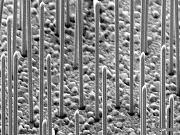
Gallium-arsenide nanowires are on a silicon surface
Data processing and transmission witnessed a much needed breakthrough with the development of the first ever photonic chip. However currently, incorporating coherent sources on a chip requires tenacious effort. Dr. Gregor Koblmüller of the Department of Semiconductor Quantum-Nanosystems at TUM joined hands with Walter Schottky and discovered a novel method to directly embed Nano lasers on a silicon chip. By adding an additional mirror on the GaAs substrate, the Silicon interface nanowire laser was transformed into a vertical cavity laser, a key step towards realising the goal of fabrication.
The team currently wants to delve deeper into the research subject before going for a commercial launch. At present, the newly discovered gallium arsenide nanowire lasers generate infrared light at a predefined wavelength and pulsed excitation. As expressed by the team, their next work will be to improvise temperature stability and light propagation under continuous excitation on the silicon chips. They would also like to devise an electric interface such that nanowires could be controlled with electrical injection, thereby eliminating the need of external laser sources.
The research was supported by the German Research Foundation (DFG), the Excellence Cluster Nanosystems Initiative Munich (NIM) and the International Graduate School of Science and Engineering (IGSSE) of the TUM, IBM. Their work was published in both the Nano Letters journal and the Applied Physics Letters journal.
Source: #-Link-Snipped-# | #-Link-Snipped-#
Proving Moore’s law wrong, electronic circuits have reached the optimum point of miniaturization and gives saturated results when it comes to further reduction of the size of contemporary transistors. Jonathan Finley, Director of the Walter Schottky Institute at TUM explained that in order to counter stagnancy in innovation, it was essential to replace electrons by photons.
Gallium-arsenide nanowires are on a silicon surface
Data processing and transmission witnessed a much needed breakthrough with the development of the first ever photonic chip. However currently, incorporating coherent sources on a chip requires tenacious effort. Dr. Gregor Koblmüller of the Department of Semiconductor Quantum-Nanosystems at TUM joined hands with Walter Schottky and discovered a novel method to directly embed Nano lasers on a silicon chip. By adding an additional mirror on the GaAs substrate, the Silicon interface nanowire laser was transformed into a vertical cavity laser, a key step towards realising the goal of fabrication.
The team currently wants to delve deeper into the research subject before going for a commercial launch. At present, the newly discovered gallium arsenide nanowire lasers generate infrared light at a predefined wavelength and pulsed excitation. As expressed by the team, their next work will be to improvise temperature stability and light propagation under continuous excitation on the silicon chips. They would also like to devise an electric interface such that nanowires could be controlled with electrical injection, thereby eliminating the need of external laser sources.
The research was supported by the German Research Foundation (DFG), the Excellence Cluster Nanosystems Initiative Munich (NIM) and the International Graduate School of Science and Engineering (IGSSE) of the TUM, IBM. Their work was published in both the Nano Letters journal and the Applied Physics Letters journal.
Source: #-Link-Snipped-# | #-Link-Snipped-#
0